


Pivector Labs
Fast atomic-scale 3D metrology for semiconductor wafers.
FOUNDED
2026
INDUSTRY
Hardware
TEAM SIZE
2
COMPANY WEBSITE
Request an intro →
About
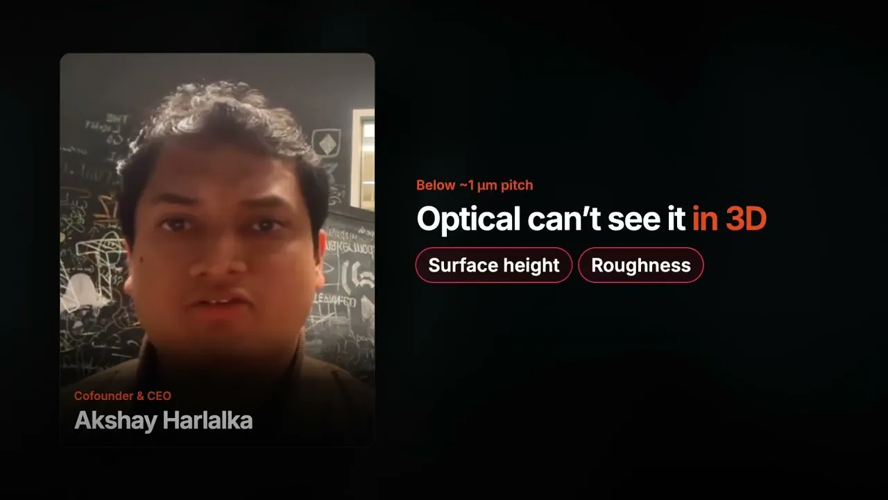
Pivector Labs develops high-throughput nanoscale 3D metrology equipment for advanced semiconductor manufacturing. Its working prototype uses atomic force microscopy to measure critical surface features on wafers with nanometer precision; the precision mechanical systems, sensor electronics, motion control and data acquisition are all built in-house.
Media
Want to join our portfolio?
If you have an idea you are excited about that fits our ethos, start an application. One of our team members will get back to you within a month.